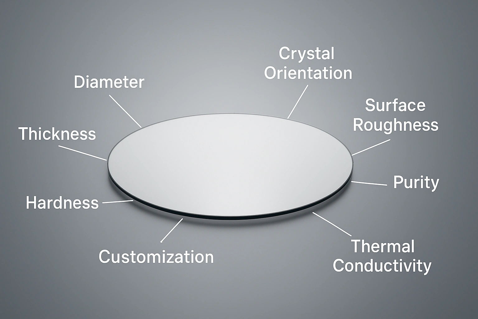
Technical Specifications

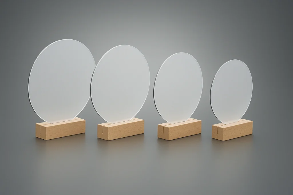
- Diameter
2 mm – 100 mm (custom on request) - Thickness
0.3 – 1.5 mm (tight tolerance) - Crystal Orientation
<100>, <110>, <111> - Surface Roughness
< 5 nm RMS (polished)
- Thermal Conductivity
> 2000 W/m·K - Hardness
~100 GPa (Vickers) - Purity
Nitrogen‑free (< 1 ppm), low defect density - Customization
Edge shaping, patterning, and application‑specific specs available
About Us

Pioneering the Future with CVD Single-Crystal Diamond Wafers
At the frontier of materials science, single-crystal diamond wafers are redefining what’s possible.
Our advanced Chemical Vapor Deposition (CVD) technology produces wafers with unmatched purity, durability, and optical clarity, tailored for the most demanding applications.
Unlike natural diamond, CVD-grown wafers are engineered for precision and scalability, enabling breakthroughs in lasers, quantum computing, electronics, and biomedical tools.
We are driven by innovation—pushing boundaries to deliver solutions that are as reliable as they are revolutionary.


